| Home | Forums | What's new | Resources | |
| Saturn USB Mod |
| Knight0fDragon - Jun 13, 2025 |
| 1 | 2 | Next |
| Knight0fDragon | Jun 13, 2025 | |||
What chips are not allowed? You do not need the parts that deal with the game storage, you just need the parts that handle the USB | ||||
| Solitario | Jun 13, 2025 | |||
So I only need this components U8, 74LS154, 74HCT245 ? | ||||
| Knight0fDragon | Jun 27, 2025 | ||
| Finally got all the parts needed for this, next step is to assemble. | |||
| Knight0fDragon | Jun 28, 2025 | |||
Doc says it writes to the transfer buffer when it goes from high to low. Wouldn't that mean I need to make it low to send the data. Not sure if I need to worry about the IRQ lines as I do not want the USB to be affected by it, and the address should disable it. Netlink's XBand library does not use the IRQ, only the dialup portion does. | ||||
| Waterfuell | Jun 29, 2025 | ||||||
Maybe it means the data is not written to the buffer until the write line goes low, or on the falling edge of the write signal. But to start the write cycle, you need to set the signal high first. Try to look for a timing diagram in the documentation.
Maybe you're right , you are controlling the CS, WR, and RD signals, which are good indicators to determine whether the bus is being used in read or write mode. | |||||||
| antime | Jun 29, 2025 | ||||||||||||||||||
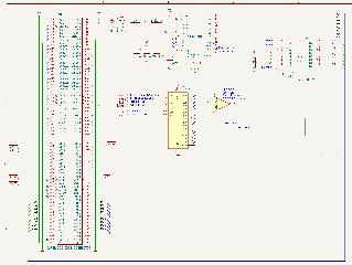
Are you sure the decoding is correct? This is what you have:
Placing PWREN on bit 7 is a small wart - because of the automatic sign extension it means you can't do MOV.B R0, .../TST #PWREN, R0, you have to add an EXTU.B R0, R0 in between. It really doesn't matter, but it still annoys me that I didn't think of it at the time. | |||||||||||||||||||
| antime | Jun 29, 2025 | |||
The decoder has inverted outputs, i.e. they idle high. | ||||
| antime | Jun 29, 2025 | ||
| Oh, don't forget the quirk that the SCU always does a 32-bit read, regardless of the access size (it is documented, but I forget in which manual). That's why I had to add the OR with A0 for the FIFO read to prevent it from being read twice for each actual read instruction. | |||
| Knight0fDragon | Jun 30, 2025 | ||||||
I think I read this table backwards. so for now I can flip the order of the pins while I test this out, and update the drawing later. 
Good call, so I should move it to bit 6. | |||||||
| Knight0fDragon | Jun 30, 2025 | |||
so what you are saying is 2 reads are always done 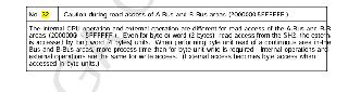 When you say A0, did you mean A1? I notice on your KiCAD files your address lines does not match the service docs, and the actual A0 is missing. Should I OR A1 and A12 together before it goes to E1? Edit: I should OR A1 and RD together. | ||||
| antime | Jun 30, 2025 | |||
It's been a while since I looked at this, but the A-bus is a 16-bit bus and the addresses are word addresses so you have to mentally shift SH-2 addresses to map them into the A-bus space. When writing to the bus, the /AWR0 and /AWR1 lines select which bytes of the word should be written. There's only one read signal, because the reader can select the bytes itself. I guess only using /AWR0 is another buglet in my design - when writing to the flash you must write in word units, you can't separately program the halves. | ||||
| Knight0fDragon | Jun 30, 2025 | |||
The flash portion is one I am actually not interested in, so I am guessing I am good on this part as the FT245RL is only written in bytes. I am guessing A0 then in this case (the service manual schematic) is always going to be low because of how the SCU is reading and writing. | ||||
| antime | Jun 30, 2025 | |||
Because SCU is reading two consecutive words, AA0 (A-bus address line zero) will be low and high. I don't know if it reading a 32-bit aligned long word, or just ADDR and ADDR+1. | ||||
| Knight0fDragon | Jun 30, 2025 | |||
I am pretty sure what you are calling AA0 is AA1 Your pinout: 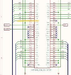 vs Sega Service Manual. 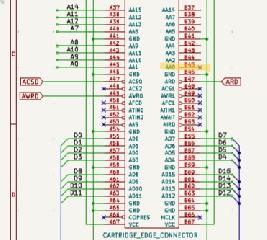 In this case, AA0 is always low as it is always 16bit reads and writes, and AA1 is what flip flops from 0 and 1 because of it being 32 bit reads. So I need to disable reading when AA1 is high to prevent the second 16bit reading. Also, no mental shifting is necessary as the address lines should line up. | ||||
| Waterfuell | Jun 30, 2025 | ||||||
Seeing that all my assumptions have been wrong, I don’t really dare to give an opinion XD. Still, you should take a look at the following post from srg320 A-Bus CS2... It seems that with A19 you can define a memory range where the double read doesn’t occur, or at least that’s what I think I understood. | |||||||
| Knight0fDragon | Jun 30, 2025 | |||
This explains why the AA19 pin is not on Netlink or XBAND modems, but AA19 is used! So I should be able to avoid said OR. | ||||
| 1 | 2 | Next |